Significantly Improve Performance and Efficiency! Ushering in the Era of Communication Chips
With the rapid development of big data and the Internet of Things, the demand for communication base stations and data centers is growing exponentially. To adapt to the rapid development of communication equipment and data centers, DC-DC power management chips must not only provide stable power output but also feature high power density, high conversion efficiency, and lower energy consumption. Therefore, DC/DC power chips with high power density, high efficiency, and high stability have become a key factor in ensuring the performance and reliability of communication base stations.
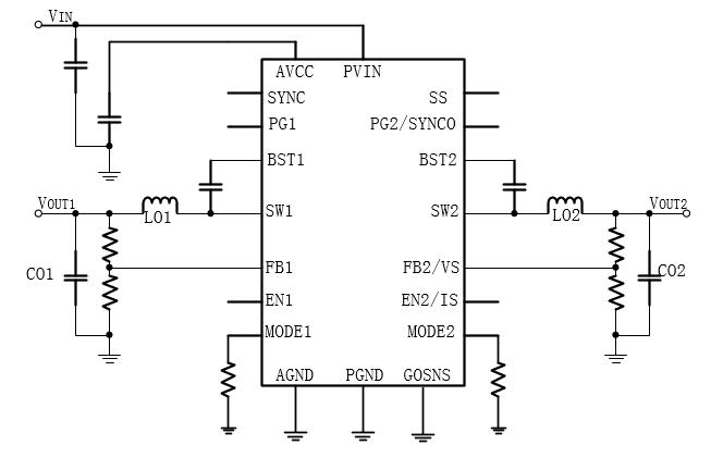
IVS introduces the highly integrated, non-isolated, dual-output DC-DC converter – IS6620A. Through optimized circuit design, improved wafer production processes, and the adoption of the most advanced packaging technology, this chip achieves higher power density and conversion efficiency, stronger anti-interference capability, and more stable output voltage. The device supports a wide input voltage range (4.5V-18V) and can be configured as two independent dual 6A outputs or a single dual-phase 12A output. Its features are as follows:
- Pseudo-Current Control Mode with internal compensation
- Dual outputs with up to 6A output current each
- Single dual-phase output with up to 12A output current
- Output voltage range: 0.5V to 5.5V, 90% maximum duty cycle
- Use SYNC to synchronize to an external clock
- Selectable switching frequencies: 500KHz, 1MHz, 1.5MHz, and 2MHz
- Two mode selection pins (MODE1 and MODE2) for selecting switching frequency, configuration, clock phase delay, and internal compensation
- Supports safe pre-bias startup
- Integrated protection functions include OCP, NOCP, OVP, UVP, OTP, soft-start protection, etc.
- 3 mm x 5 mm, 25Pin FC-QFN package
Technical Features
- Simple control loop with strong anti-interference capability
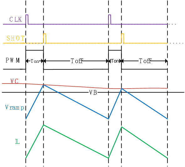
Figure 2 shows a simplified schematic of the Pseudo-Current Control Mode (PCC), and Figure 3 shows its timing diagram. The input Vramp to the PWM comparator is generated by the Pseudo Current module, not directly sampled from the inductor current. It has a waveform similar to the inductor current IL, as shown in Figure 3. When the CLK signal arrives, the PWM signal goes high, turning on the high-side power MOSFET. Vramp rises linearly like the inductor current. When it reaches VC, the PWM flips, generating a SHOT signal, the PWM goes low, turning off the high-side FET and turning on the low-side FET until the next CLK arrives. PCC achieves fast dynamic response through nonlinear slope compensation techniques (Vslp+ and Vslp-). Furthermore, a unique VC clamping technology enables smooth voltage transition between DCM and CCM.
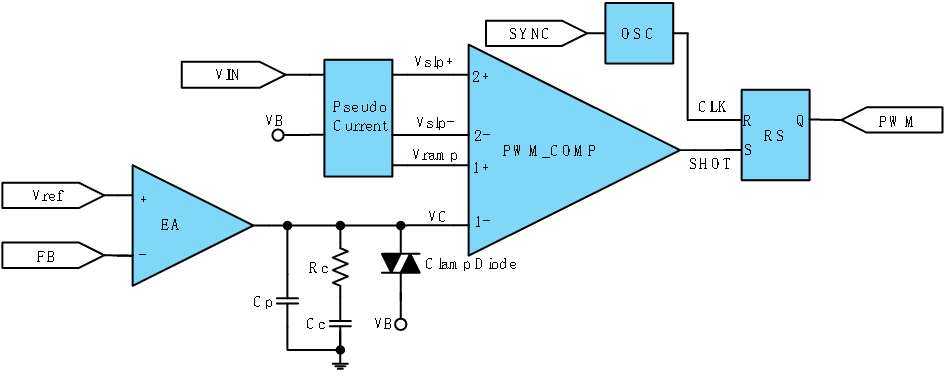
Compared to traditional peak current control mode, PCC offers better anti-interference capability, a shorter minimal on-time, and can achieve extremely low jitter. The advantage in anti-interference is particularly significant under high current conditions. Compared to COT control mode, PCC uses a fixed frequency (CLK from internal OSC or external SYNC signal), which is beneficial for synchronizing dual-phase parallel operation and stable phase control.
- External CLK synchronization function further enhances system anti-interference capability
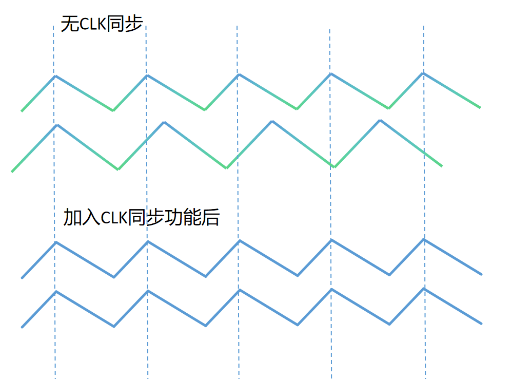
When multiple switching power supplies operate at different frequencies, they can cause electromagnetic interference with each other and affect the normal operation of other electronic devices. Synchronizing switching frequencies aligns the output voltage and current waveforms of multiple power supplies, reducing mutual interference and thereby improving system anti-interference capability. When the SYNC pin of the IS6620A chip receives a system CLK signal, in MR1 mode and when a 50% duty cycle CLK signal within ±20% of the frequency set by the Mode pin is input, the IS6620A's operating frequency synchronizes with the external CLK. If the SYNC signal remains high, low, or floating, the operating frequency is determined by the CLK generated by the internal OSC, with SW1 and SW2 operating with a 180° phase shift.
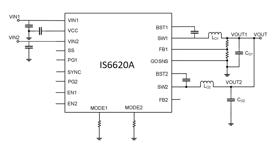
The following is a configuration example for a dual-phase single-output power supply synchronized to an external CLK:
- The two Vouts of the chip are connected together.
- The switching frequency is set by the external CLK received at the chip's SYNC pin.
- The 2-phase shift is set by the chip's Mode pin.
- The GOSNS pin serves as the input for remote sensing.
- Built-in integrator ensures high output voltage accuracy
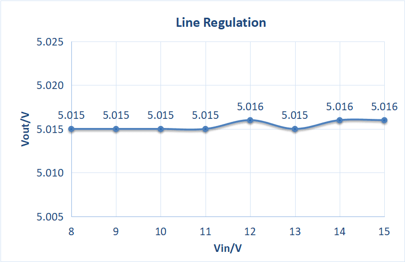
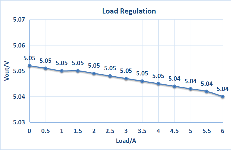
The IS6620A chip incorporates an integrator function that continuously corrects the reference voltage Vref, thereby improving voltage accuracy under varying load and input voltage conditions. The output voltage accuracy reaches up to ±1%.
- High efficiency and low power consumption
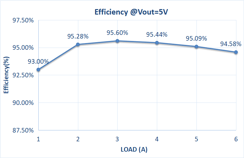
The chip integrates MOSFETs with low on-resistance Rdson (20mΩ/8mΩ HS/LS) and optimized drive current technology. The IS6620A achieves a peak efficiency of 95.6% under Vin=12V, Vout=5V conditions. Under light load conditions, when the chip operates in DCM mode, it can further reduce power loss and improve overall system efficiency.
Application Scenario Example
The input voltage for communication equipment is typically -48V. This is first converted to 12V via an isolated DC/DC converter, then converted to the voltages required by the mainboard chips via non-isolated DC/DC converters. The following introduces a power supply application design example using IS6620A:
Application conditions: VIN=12V, VOUT1=1.2V (Imax=6A), VOUT2=1.0V (Imax=6A), Load Step: 0A~3A & 3A~6A, Vpeak-peak of VOUT1 ≤120mV (±5%), Vpeak-peak of VOUT2 ≤100mV (±5%).
First, select the switching frequency. IS6620A offers 500KHz, 1MHz, 1.5MHz, and 2MHz. A frequency of 1MHz is generally recommended.
Next, determine the inductance. Select a value based on an inductor current ripple of 20%~40% of the full-load output current. For this application with a full-load current of 6A, the ripple range is 1.2A~2.4A. Using the formula $\mathrm{\Delta}IL = \frac{VIN - VOUT}{L} \ast T_{ON}$, with VOUT=1.2V, Fsw=1MHz, calculation yields an inductance range of 0.45uH~0.9uH when VIN=12V. For VOUT=1.0V, Fsw=1MHz, VIN=12V, the inductance range is 0.38uH~0.76uH. Finally, an inductance of 0.47uH is chosen for both.
Finally, based on the design tool provided by IVS, suitable output capacitors are selected for the 1.2Vout and 1.0Vout. For Vout=1.2V, six 22uF ceramic capacitors are used; for Vout=1.0V, six 22uF ceramic capacitors are used. With this, the key parameters for this application are determined. The corresponding measured waveforms are shown below.
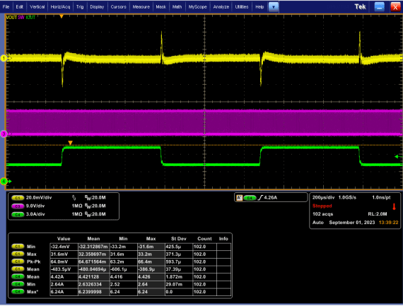
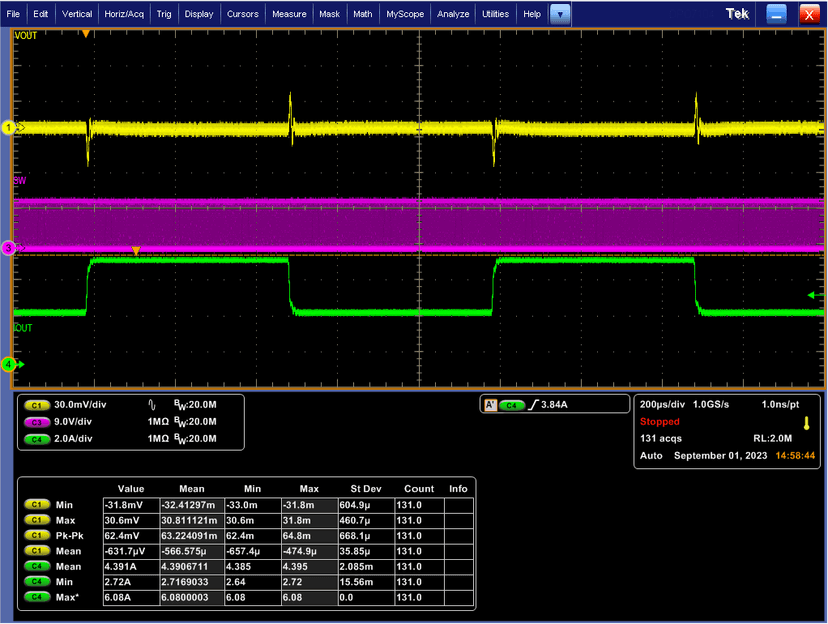
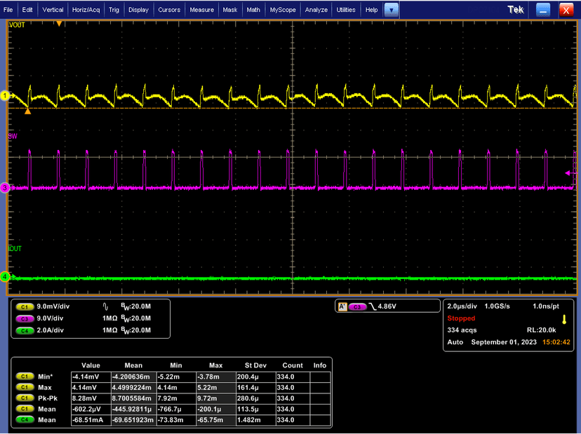
Transient: VIN=12V, VOUT1 =1.2V, LOAD Step=3A , Slew rate=1A/µs, Vpeak-peak=66.4mV
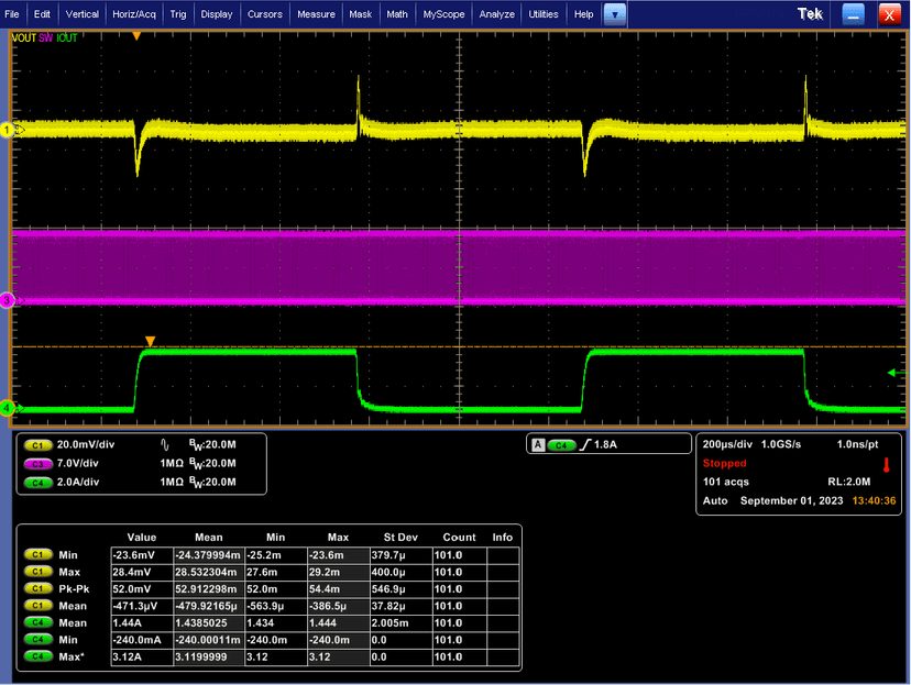
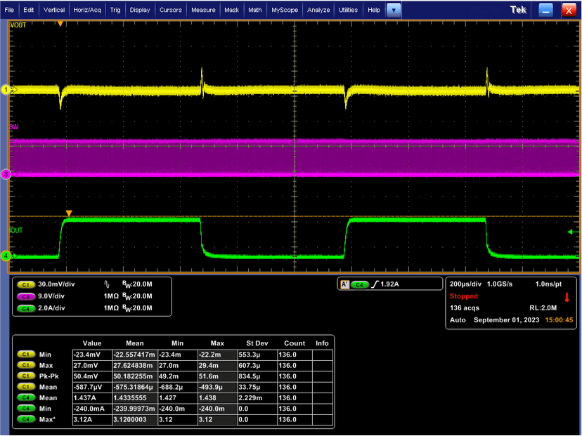
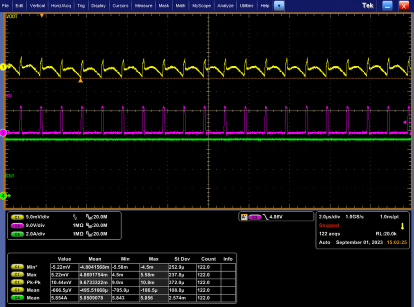
Transient: VIN=12V , VOUT2=1.0V, LOAD Step=3A , Slew rate=1A/µs, Vpeak-peak=64.8mV
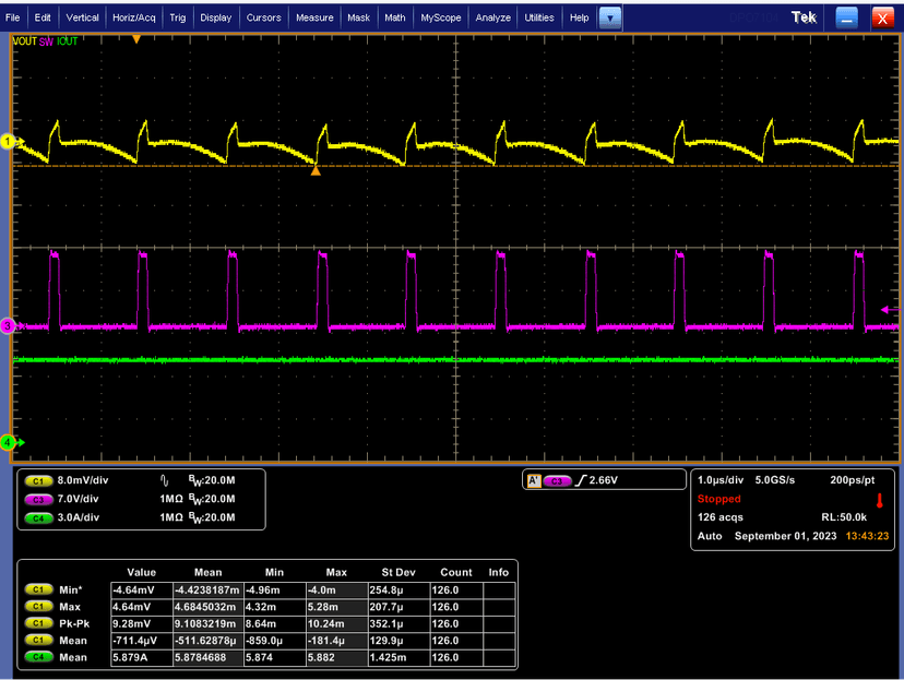
Ripple: VIN=12V, VOUT1 =1.2V, LOAD=0A,6A Vripple=10.24mV
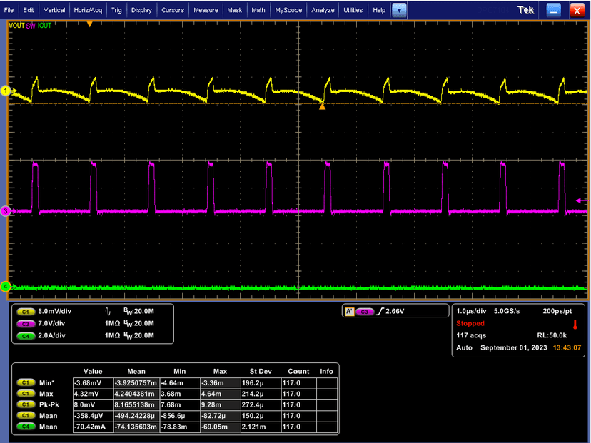
Ripple: VIN=12V, VOUT2 =1.0V, LOAD=0A,6A Vripple =10.8mV
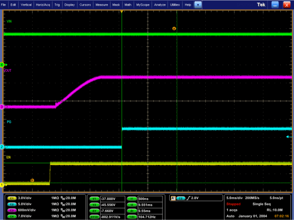
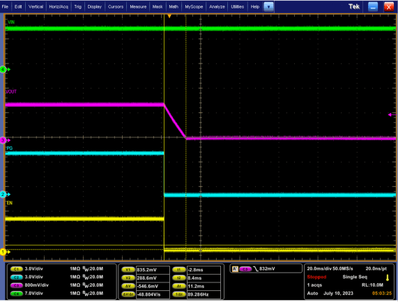
Vout1 Power on and off by EN
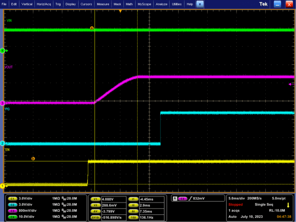
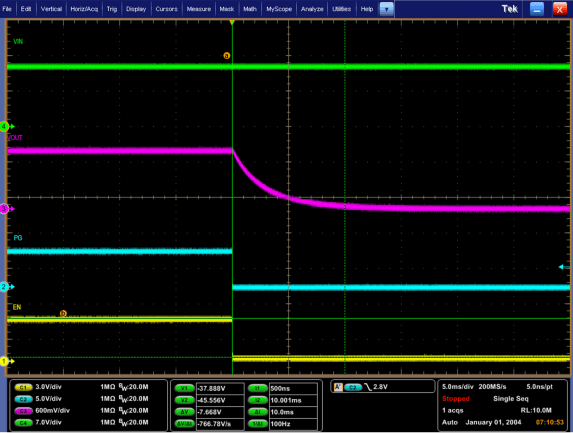
Vout2 Power on and off by EN