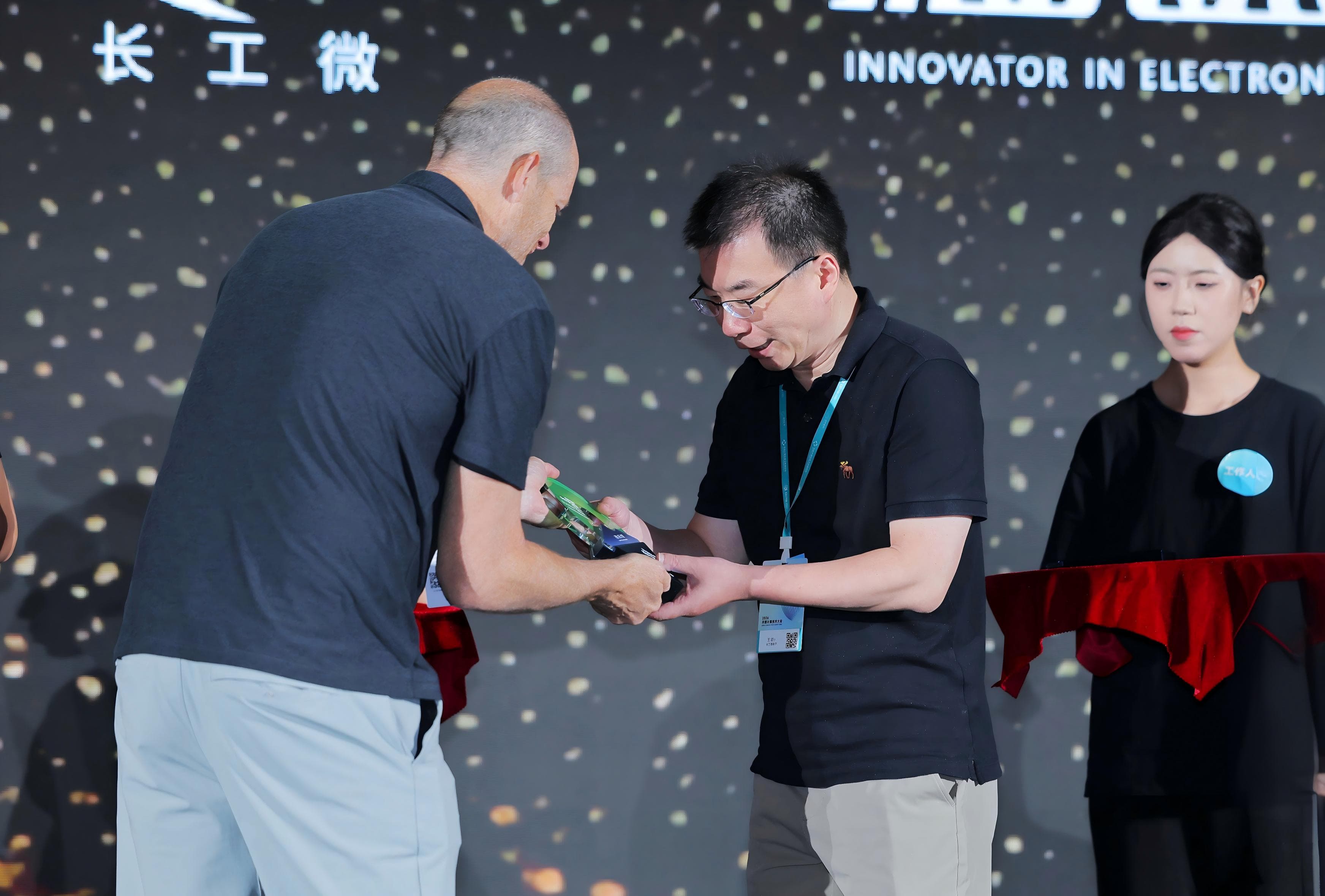
IVS Shines at 2026 Open Computing Technology Summit, Wins Innovation Award
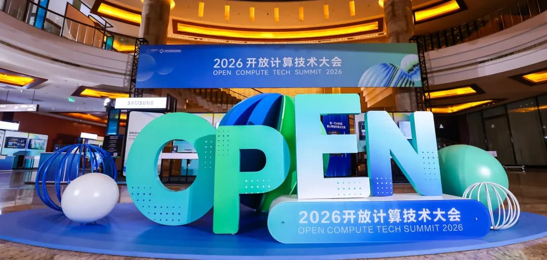
The 2026 Open Computing Technology Summit (OCTS 2026), themed "Intelligent Computing Beyond Boundaries | Open, Diverse, Scalable," concluded successfully in Beijing.
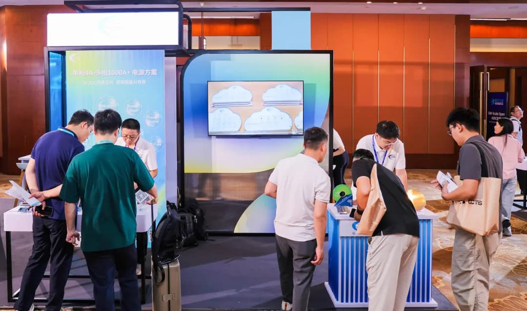
IVS showcased its full suite of computing power hardware system-level power supply solutions at the summit and won the Open Computing Best Innovation Award for its self-developed chip—IS6214A. In addition, the company's technical experts delivered keynote speeches, engaging in in-depth discussions with industry chain partners on the evolution and implementation paths of data center power supply technology amid the surge in AI computing power.
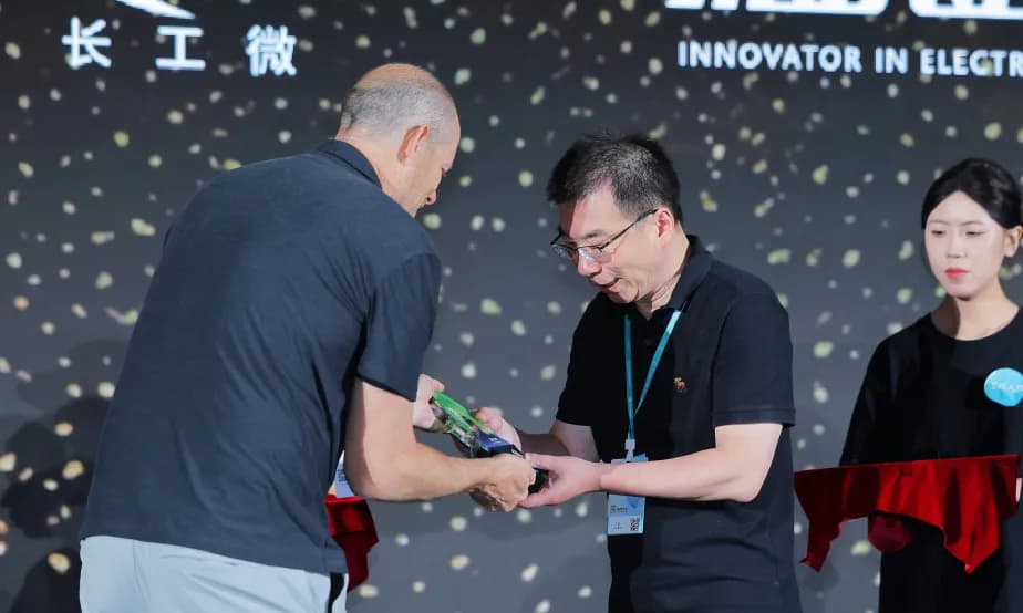
Strength Recognized! IS6214A Wins Open Computing Best Innovation Award
During the prestigious award ceremony at the summit, IVS's dual-loop hybrid analog-digital 16-phase PWM controller—IS6214A stood out and won the Open Computing Best Innovation Award, thanks to its three core advantages: leading load transient regulation, high-precision multi-phase current sharing and reliability, and full-scenario platform compatibility. The core technology received high recognition from industry authoritative reviewers.
IS6214A is a high-end VRM system intelligent control hub for AI server computing power supply. It can drive up to 16 interleaved DrMOS phases to achieve kiloampere-level large current output, efficiently converting the 12V bus voltage to a core operating voltage of 0.5V~3.2V.
The product adopts the self-developed TCOT™ control architecture, achieving fast response with up to 5MHz switching frequency per phase PWM under a load transient of 1000A/μs. The output slew rate is programmable from 1mV/μs to 50mV/μs, and it features a built-in output voltage compensation mechanism to effectively suppress overshoot and undershoot during dynamic load transitions, ensuring power supply stability. Additionally, the chip integrates a digital phase-locked loop (PLL) module to precisely synchronize multi-phase PWM switching, reducing ripple and simplifying system filter design.
In terms of compatibility and reliability, the chip supports PMBus, AVSBus, and PWM-VID communication protocols. It enables high-precision current sampling in both DrMOS built-in Imon and inductor DCR modes, monitors the Power Stage operating temperature in real time, and dynamically adjusts PWM output to limit temperature rise. The chip integrates a full set of protection mechanisms including overvoltage, overtemperature, phase current balance, and overcurrent, precisely matching the high dynamic load power supply scenarios of AI computing chips.
Keynote: Three Generations of Power Supply Architecture Evolution Addressing Core Computing Power Challenges
Currently, new-generation XPUs such as GB300 and Feynman are experiencing skyrocketing power consumption, with peak currents exceeding 2000A and transient current slew rates reaching 10000A/μs. The performance upgrade of computing hardware imposes stringent requirements on power supply transient response and voltage tolerance. The core optimization direction is to reduce the output inductance Lout of the power supply system, lower the bus voltage, and increase the Ton time, enabling the VR power supply to quickly replenish load current demand.
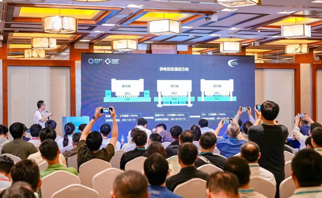
At the summit's Computing-Power Synergy Development Forum, IVS delivered a keynote speech titled "Development Trends of Multi-Phase Power Supply Solutions in Data Centers," comprehensively sharing three generations of iterative technology routes: horizontal power optimization, vertical power delivery, and IVR forward-looking layout, providing a full-cycle computing power supply solution for the industry:
● Optimizing 12V Board-Level VRM Horizontal Power Supply
The traditional board-level horizontal power supply bus evolves to 48V-12V-1V, with an operating frequency of about 1MHz. Affected by PCB trace resistance, system conduction losses are high under large current conditions. For a 2KW XPU device, the trace loss (R1 Loss) reaches up to 400W, severely limiting overall system energy efficiency.
To meet the computing power upgrade needs in data centers, IVS leverages customized processes to continuously iterate multi-phase controllers and smart power stage solutions, reducing system losses and fully exploiting the potential of the 12V power supply architecture. Among them, the 12V high-current dedicated power device IS6812A can deliver 70A output current, with Rsp reduced by 12%, FOM reduced by 22%, and UIS improved 15 times compared to similar products. Its maximum withstand current exceeds 200A, offering excellent conversion efficiency and robustness, stably supporting long-term full-load operation of 2000W+ mainstream AI accelerators.
● Implementing 5V Vertical VPD (Vertical Power Delivery)
The vertical VPD power supply architecture increases the operating frequency to 3MHz, with the bus voltage evolving to 48V-6V/5V-1V. By placing the power module close to the XPU, the power path is shortened, reducing transmission losses. For the same 2KW XPU, the trace loss of the vertical power delivery solution (48V-6V-1V) drops from 400W to 26W, and the system power reduces from 2727W to 2291W.
As the first domestic company to implement a complete 5V vertical power delivery technology route, IVS optimizes power density and conversion efficiency from the architecture bottom layer using advanced processes. The self-developed IS6815A 5V smart power stage adopts a single-chip integration, supporting 90A/120A large current output, with UIS capability enhanced 90 times compared to standard 5V power transistors and FOM optimized by over 30% compared to discrete MOS devices. In addition, IVS has launched several high-frequency, high-current DrMOS products, such as the IS6825A, which operates at up to 3MHz and delivers a maximum output current of 110A. These products are fully compatible with vertical power module designs, breaking the power bottleneck of ultra-high-power computing cards and supporting the construction of large-scale intelligent computing centers.
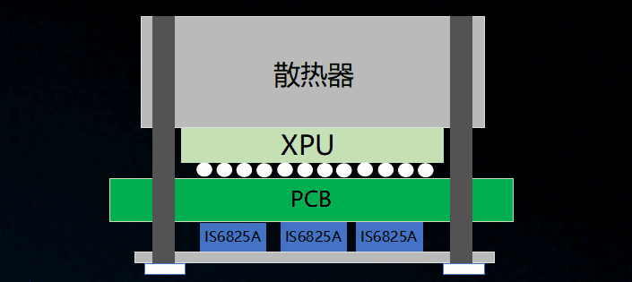
● Layout of IVR Architecture—Bridging the Last 1mm
Looking ahead to ultra-high-density computing scenarios, the industry's power supply architecture will evolve to a 48V-3.3V-1V chip-level IVR (Integrated Voltage Regulator) solution. This architecture features ≤3.3V, >10MHz, high power density, and an ultra-thin power supply design, precisely addressing core challenges such as partitioned power supply for high-end XPUs and dynamic energy efficiency optimization. It is the optimal technical path for future computing power supply. IVS will develop self-developed high-frequency voltage regulator chips covering an operating frequency range of 1MHz~10MHz, matching ultra-high current slew rate conditions, and fully supporting the R&D and deployment of next-generation low-voltage, high-frequency IVR power supply architectures.
Looking ahead, IVS will continue to deepen its focus on the core field of AI data center power supply, continuously iterating full-stack computing power supply solutions. The company looks forward to joining hands with industry peers, experts, and partners to pool efforts and collaborate on innovation, perfecting the underlying infrastructure of computing hardware, and jointly building an efficient, low-carbon, and intelligent open computing ecosystem to support the sustainable development of the AI computing power industry.